Capturing electrons on their trip between atoms
Electrons require tens to hundreds of attoseconds to travel between neighbouring atoms in solids.
Electrons require tens to hundreds of attoseconds (1 as = 0.000 000 000 000 000 001 second) to travel between neighbouring atoms in solids. While astonishingly brief, these attosecond travel times will ultimately limit the speed of electronics in the future. Advancing technology toward this ultimate limit will rely on the capability of real-time measurement and finally, control of electron transport in solids with attosecond resolution. Recently, in the Laboratory of Attosecond and High-Field Physics (www.attoworld.de) at the Max Planck Institute of Quantum Optics, an international team of researchers, Adrian Cavalieri from the USA along with his coworkers from Austria, Hungary, Germany, and Spain achieved the first of these goals by measuring the difference between the travel times of two different types of electrons through several atomic layers. The experiment constitutes the first attosecond measurement in condensed matter and opens the door to control of electron transport in solids on the atomic scale. The accomplishments are reported in Nature on October 25, 2007 and highlighted on its cover.
The controlled transport of electric charge by electrons through nano-scale electric circuits forms the basis of modern electronics, used, for example, in computers, communication devices and measuring instruments. Motivation for developing faster electronics comes from many directions: faster computers and more sensitive instruments will allow more reliable prediction of natural disasters and deeper insight into the workings of nature by ever more sophisticated modelling; ultrahigh-speed communication systems may, one day, permit specialists to perform remote surgery and will make healthcare more efficient in many other ways, to mention only a few of many possible implications.
In state-of-the-art electronic circuits, electrons are driven by a microwave voltage, which is capable of switching on and off current within a fraction of a nanosecond (1 ns = 1 billionth second = 0.000 000 001 second). The switching time determines the number of calculations that can be performed by a computer clocked by this chip during a certain period of time. Ultimately, the rapidity of switching is limited by the time it takes for the electrons to travel through the structures used for guiding and controlling their current. Smaller structures lead to faster switching speeds and a higher density of information flow. The quest for ever smaller nanostructures in solid-state electronics and for atomic assemblies in molecular electronics is driven by these simple considerations. The distance between neighbouring atoms in a crystal lattice or in a molecule constitutes presumably the smallest possible length scale for channelling and switching current for the purpose of information processing. The time it takes for electrons travelling distances on the atomic scale is naturally clocked in attoseconds (1 as = 1 billionth of one billionth second), implying the potential of switching electric current more than a trillion times in atomic-scale (solid-state or molecular) circuitry. This would result in the emergence of Petahertz electronics, in which the direction of electric current can be changed at a rate of several trillion times per second, some hundred thousand times higher than permitted by present-day electronics.
A first essential step on the long way towards ultimate-speed electronics, limited only by the time required for an electron to travel between neighbouring atoms, is the development of techniques to capture electronic charge transport in atomic-scale structures on the attosecond time scale. This first step was recently successfully demonstrated in a proof-of-principle experiment at the Max Planck Institute of Quantum Optics (MPQ) in Garching, Germany, in which researchers observed attosecond electric charge transport across several atomic layers near the surface of a crystalline solid in real time [1].
The team of MPQ researchers along with their coworkers from the Universities of Bielefeld, Hamburg and Vienna shone a 300-attosecond pulse of extreme ultraviolet light along with an infrared laser pulse comprising a few, well-controlled oscillation cycles of its electric field on the surface of a tungsten crystal. In a sequence shown in Figure 1, the attosecond pulse penetrates the tungsten crystal, and particles of extreme ultraviolet light, henceforth briefly photons, are absorbed, which results in freeing both loosely-bound electrons, responsible for conduction, and electrons bound tightly to the cores of the atoms forming the crystal lattice. These electrons are excited simultaneously and speed from a depth of several atomic layers, to the surface, at a different speed: the loosely-bound (conduction) electrons travel faster than the tightly-bound (core) electrons. Once at the surface, the electron’s initial velocity, which depends on the energy of the absorbed photon and the electron’s original binding energy (as predicted by Einstein more than a century ago), is changed by the electric field of the incident laser pulse and this change can be detected by a time-of-flight detector. This measurable change depends on the instant of arrival of the electron on the crystal surface and varies significantly with the laser field as it varies during its oscillation (the half cycle of which takes 1250 attoseconds). From the measured changes in the slow and fast electrons’ initial velocity attosecond-scale differences in the arrival time of the electrons can be unambiguously determined.
By changing the electrons’ velocity in a controlled fashion, the rapidly oscillating laser field serves as a stopwatch with attosecond resolution, revealing that the conduction electrons reach the “finish line”, i.e. the crystal surface, some 110 attoseconds earlier than the core electrons. This difference in arrival time on the surface indicates that, inside the tungsten crystal, the freed conduction electrons travel twice as fast as those originally localized near the atomic cores. The MPQ experiment demonstrates the technical capability of measuring electronic charge transport across atomic layers in real time with attosecond temporal resolution. Future measurements of this type will allow for research into structures and technologies for speeding up state-of-the-art electronics by several orders of magnitude.
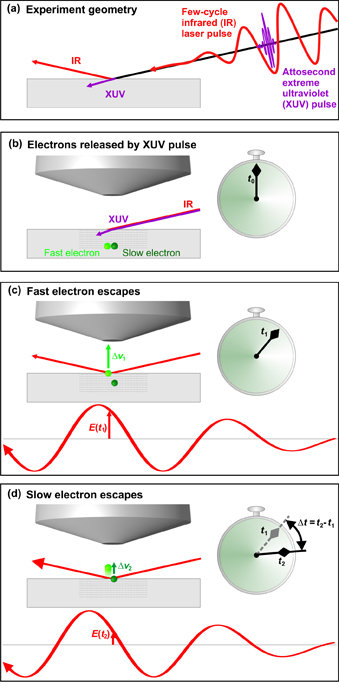
Fig. 1: Frame-by-frame overview of the MPQ experiment.
In panel (a), an infrared (IR) laser pulse comprising a few well controlled oscillations of its electric field (red line) and an attosecond extreme ultraviolet (XUV) pulse are incident on a tungsten crystal. The IR pulse is primarily reflected from the surface and the XUV pulse penetrates the crystal.
In panel (b), the attosecond XUV pulse is absorbed in the crystal, setting free two types of electrons: fast electrons responsible for conduction, and slow electrons originating from the vicinity of the atomic cores. The electrons being freed in this fashion within several layers below the crystal surface have the chance for reaching the surface without energyreducing collisions and escape the crystal.
Panel (c) and (d) capture the instants when the fast and slow electrons reach the surface, respectively, and are subsequently sped up by the infrared laser pulse. They reach the surface at different instants, t1 and t2 . Consequently, the electrons arriving at these instants experience significantly different strengths of the laser electric field, E(t1) and E(t2), which cause different changes in the electrons’ velocity, Δv1 and Δv2, respectively. These changes can be measured by a time-of-flight detector, from which the time elapsing between the arrival of the two types of electrons on the surface, Δt=t2-t1can be determined with attosecond accuracy. Artwork: Barbara Ferus, Ludwig-Maximilians-Universität München.
Contakt:
Prof. Dr. Ferenc Krausz
Director at Max Planck Institute of Quantum Optics
Hans-Kopfermann-Strasse 1, 85748 Garching, Germany
Chair of Experimental Physics, Ludwig Maximilians Universität Munich
Phone: +49 (0)89 32 905 -612 / Fax: -649
E-mail: ferenc.krausz@mpq.mpg.de
www.attoworld.de, www.munich-photonics.de
Dr. Olivia Meyer-Streng
Press & Public Relations
Max Planck Institute of Quantum Optics
Phone: +49 (0)89 32 905 -213
E-mail: olivia.meyer-streng@mpq.mpg.de
