Trapping light in a carbon net
Graphene, an ordered monolayer of carbon, is the thinnest substance known, and yet has extraordinary mechanical strength. A new study shows that its two-dimensional network of atoms can even trap light.
Thin, thinner, graphene. Graphene, a monolayer of carbon in which the atoms are arranged in a two-dimensional honeycomb network, is the thinnest net in the world, is highly stable. Andre Geim and Konstantin Novoselov received the Nobel Prize for Physics in 2010 for their discovery of the electrical conductivity of graphene. Indeed, graphene could in future replace silicon as the basis for extremely small and extremely fast transistors, and is therefore the subject of intense research.
The high mobility of electrons in graphene arises from the fact that they are confined to the hexagonal lattice. An international team led by the American physicist Dimitri Basov has now shown that photons too can be trapped within the lattice and move freely along it. “It is even possible to control the light waves within the lattice,” says physicist Dr. Fritz Keilmann, who is affiliated with LMU, the Center for Nanoscience (CeNS) and the Max Planck Institute for Quantum Optics (MPQ), and contributed significantly to the new work.
Computers with optical switches
Such control can be exerted using electric fields and currents. Hence, in future, the behavior of light in graphene could be tuned electrically, and the converse may also be feasible. Since the light is confined to nanocables with dimensions of a millionth of a millimeter, switching times could be reduced to less than a picosecond (0.000000000001 sec). “It might even be possible to develop computers whose graphene transistors could be switched both optically and electrically,” says Keilmann.
Theoretical calculations had previously suggested that photons, specifically long-wavelength infrared photons, could indeed be propagated along the graphene lattice at greatly reduced velocities. The slowing effect was attributed to the formation of plasmons, a type of hybrid particle produced by coupling of the photons to electronic excitations in graphene. It has not been possible to study the predicted plasmons experimentally, because the momentum of the infrared photons was far too low to excite them.
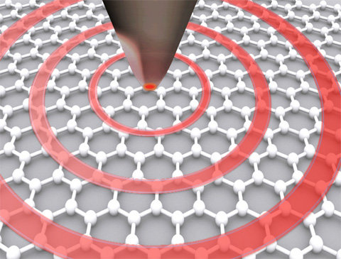
Figure: Artist's impression of how the near-field microscope's tip launches infrared plasmon waves along graphene, a single-atom carbon sheet. (Illustration: AlexanderAlUS/Fritz Keilmann)
Bringing photons to the point
This problem has now been solved with the aid of a tiny metal pin with a nanometer-sized tip. Acting like a lightning rod, it concentrates incident light into a very small volume. This raises the momentum of infrared photons by up to 60-fold, giving them the extra momentum they need to launch plasmonic waves along the graphene layer. For this purpose, the researchers made use of a commercial infrared scanning near-field microscope, whose finely honed scanning tip is normally used to map the chemical composition of a material under test
In this case only the edge zone of a graphene sample was imaged. Reflection of the plasmons at this edge produces an interference pattern, which encodes information that can be used to confirm formation of the plasmons. It also allows one to deduce many of their properties, such as the magnitude of the reflection at the graphene edge and the change in the velocity by external electric bias, which is of particular interest for future applications. “The long-sought ability to control light signals by electrical means has thus been realized,” says Keilmann.
An independent study carried out by a Spanish group, based on the use of a graphene sheet formed by deposition from the gas phase rather than the exfoliated film used in the LMU work, comes to a similar conclusion. The two papers have now appeared back-to-back in the top-tier journal Nature, underlining the significance of these findings for the field of nanoelectronics. Susanne Wedlich
Contact:
Dr. Fritz Keilmann
Phone: +49 (0)89 / 289 -14088 (-14106 lab)
Fax: +49 (0)9113 0844 88883
E-mail: keilmann@lasnix.com
Dr. Olivia Meyer-Streng
Press & Public Relations
Max Planck Institute of Quantum Optics
Phone: +49 (0)89 / 32 905 -213
E-mail: olivia.meyer-streng@mpq.mpg.de